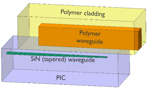
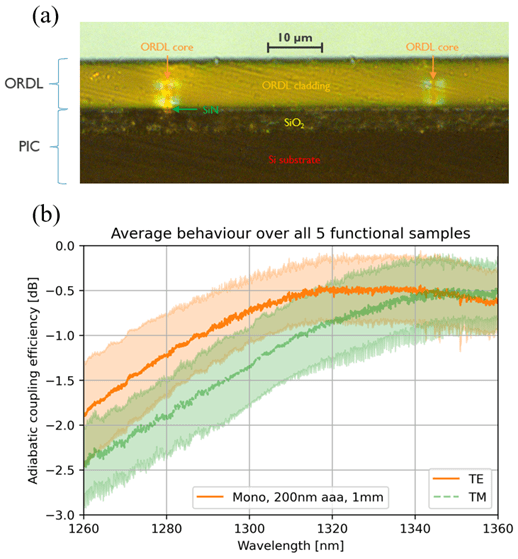
Low-loss PIC-to-ORDL adiabatic coupling
IMEC developed an efficient PIC-to-ORDL adiabatic coupling approach. The figure shows the concept, a cross-section of the realized structures and sub -1dB coupling efficiency in O band for TE and TM polarization. (ORDL: optical redistribution layer). More info.
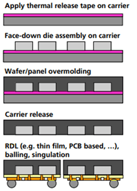
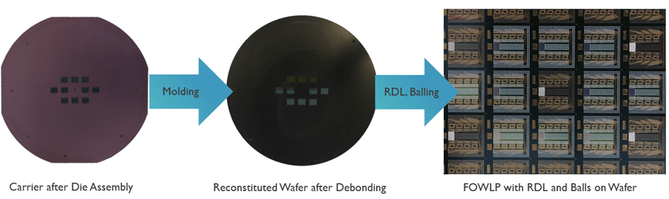
Fan-Out Wafer-Level Packaging (FOWLP) of electronic and photonic ICs
Fraunhofer IZM developed Fan-Out Wafer-Level Packaging (FOWLP) technology that allows co-packaging optical and electrical ICs on wafer level. The figure shows the process flow and results of a mock-up demonstration using dummy optical/electrical ICs.
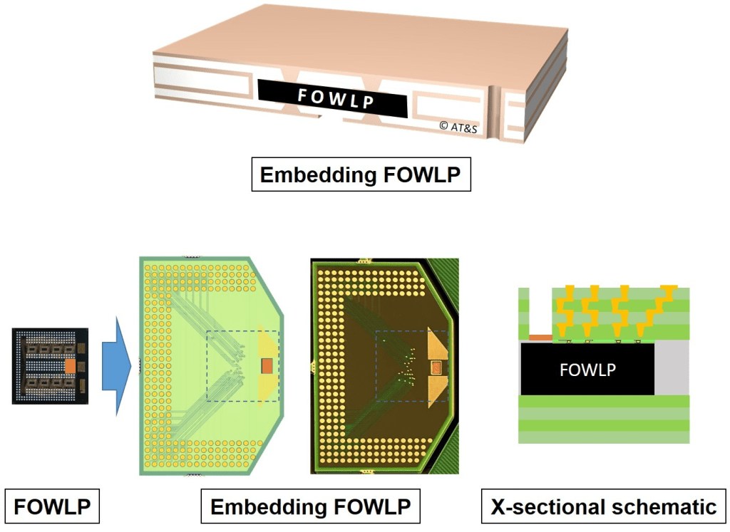
Embedding in high-density substrates
AT&S develops technology to embed Fan-out Wafer-Level Packages (FOWLP) in high-density substrates. The FOWLP’s can house both electrical and optical ICs, making the approach highly relevant for co-packaged optics.
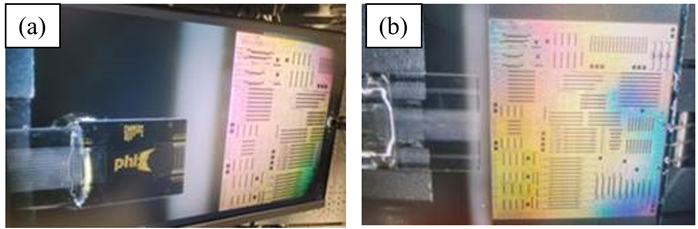
Reliable fiber array attachment
PHIX developed solutions for reliable fiber array attachment to edge couplers on embedded PICs
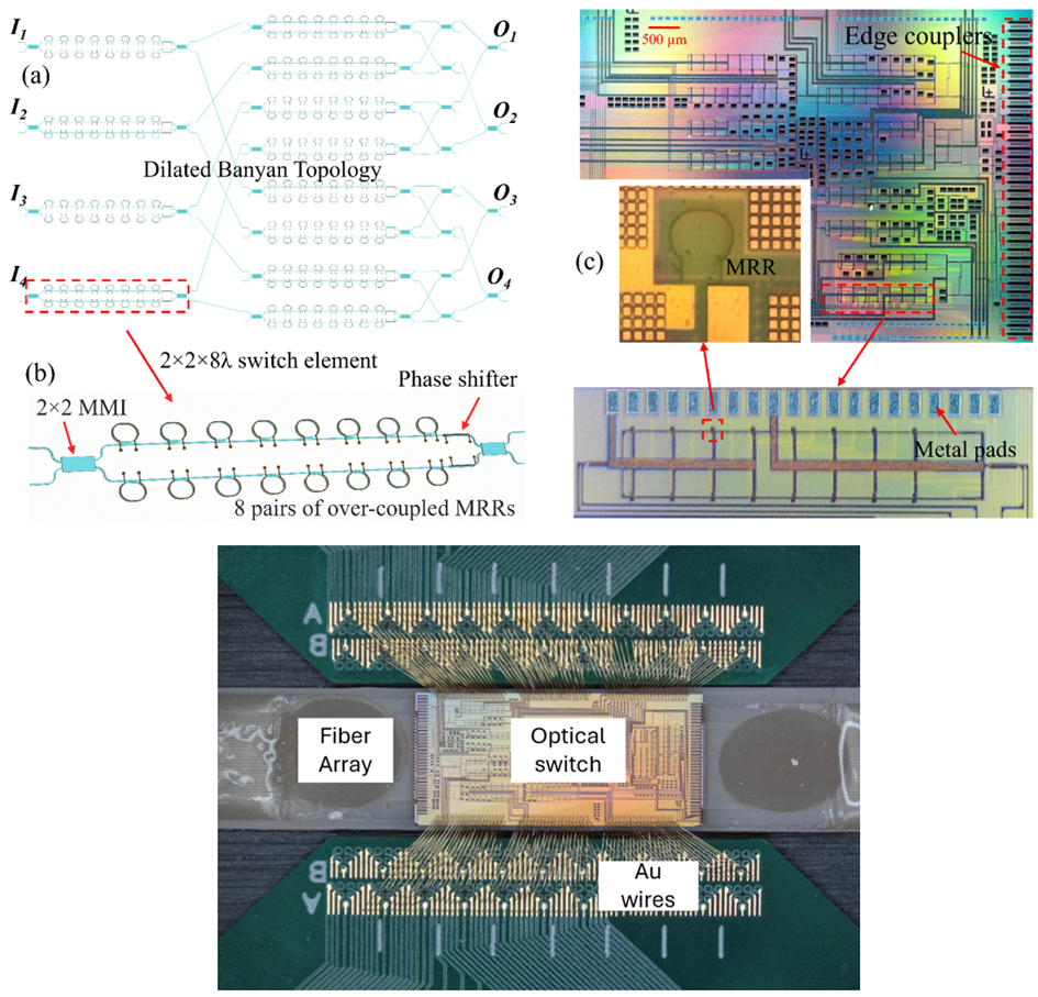
4×4×8λ space-and-wavelength selective optical switch
Cambridge University developed optical switches in a modified dilated Banyan topology, where 8 wavelength channels with 1.1 nm wavelength spacing are independently controlled through thermal tuning of microring-based resonant phase shifters. This design combines the high tuning efficiency and wavelength selectivity of microring resonators (MRRs) with the broad bandwidth and stability of Mach-Zender interferometers (MZIs).
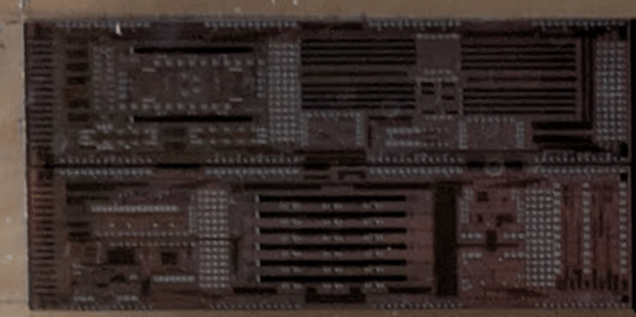
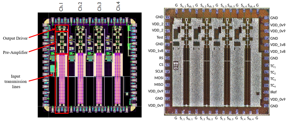
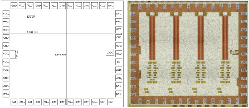
Chips for 1.6 Tb/s optical transceiver
IMEC developed a 32-channel (4 spatial channels, 8 wavelengths) transmitter and receiver PIC and matching high-speed modulator driver chips (4 Ch) and transimpedance amplifier chips (4 Ch).